
1342nm Solid-State Laser: The "Golden Light Source" for Precision Processing of Silicon-Based Semico
1342nm Solid-State Laser: The "Golden Light Source" for Precision Processing of Silicon-Based Semiconductors ✨
In the field of precision processing of silicon-based semiconductors, a light source with a unique wavelength is gaining industry favor—the 1342nm solid-state laser. With its irreplaceable technical advantages, it has become a cost-effective solution for industrial and scientific research scenarios. Today, let’s take an in-depth look at this "golden light source".
1. Why 1342nm? The Core Value of a Unique Wavelength
Silicon-based materials exhibit precise absorption characteristics to 1342nm laser light, enabling efficient material removal while minimizing the heat-affected zone and avoiding damage to surrounding precision structures. This property makes it stand out in micron-level precision processing, earning it the industry-recognized title of "golden wavelength".
Compared with traditional light sources, the 1342nm solid-state laser achieves smoother cutting edges and more uniform etching depth in silicon-based processing, providing reliable process guarantees for the manufacturing of high-end semiconductor devices.
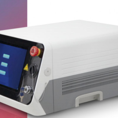
2. Four Core Advantages to Strengthen Product Competitiveness
The product features of this laser perfectly meet the demand for long-term stable operation in industrial environments:
- High reliability and long lifespan: Adopting mature solid-state laser technology, core components have a long service life and can adapt to high-intensity production environments, significantly reducing equipment replacement frequency.
- Excellent beam quality and mature technology: With a beam quality M² <1.3, it offers high focusing precision. The process stability has been verified over the long term and can be directly integrated into existing production lines.
- Capable of long-term continuous operation: Supports 7×24-hour continuous working mode, meeting the capacity requirements of large-scale production in semiconductor factories.
- Simple maintenance and low operating costs: Modular design facilitates daily maintenance, with low consumable consumption, making long-term use costs significantly lower than similar devices.
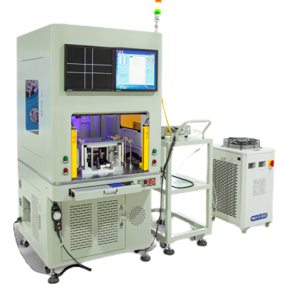
3. Diverse Application Scenarios Covering Industrial and Scientific Research Fields
🔹 Industrial Manufacturing
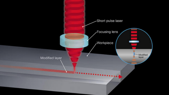
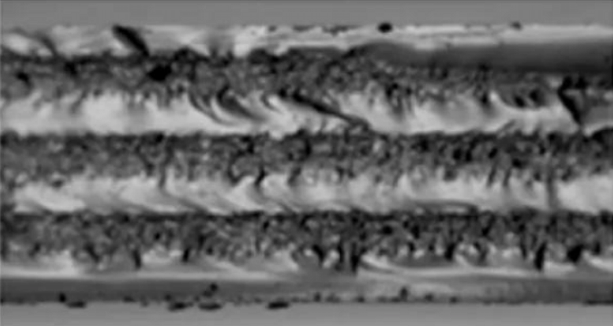
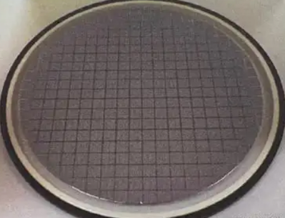
1. Silicon Wafer Stealth Dicing: Uses 1342nm laser to form a modified layer inside the silicon wafer, achieving stress-free and debris-free wafer separation, especially suitable for processing ultra-thin and large-size wafers.
2. Integrated Circuit (IC) Trimming: Performs fine-tuning on precision components such as chip resistors and capacitors to correct circuit parameters and improve chip yield and performance consistency.
3. MEMS Device Manufacturing: Achieves sub-micron precision processing in the structural etching and electrode formation of micro-electro-mechanical systems (such as accelerometers and gyroscopes).
4. Display Panel Repair: Precisely repairs pixel defects and line breaks in OLED and LCD panels to extend their service life.
🔹 Scientific Research and Medical Care
1. Biological Imaging and Diagnosis: Serves as a light source with high penetration depth and high resolution in biological imaging technologies such as optical coherence tomography (OCT).
2. Basic Optical Research: Acts as an ideal light source for spectral analysis and nonlinear optical experiments, supporting cutting-edge scientific exploration.
3. Polymer Micromachining: Enables thermal damage-free precision etching in the manufacturing of polymer microfluidic chips and microlenses.
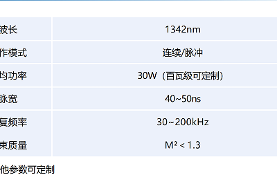
4. Key Technical Parameters Supporting High-End Applications
Parameter Item Specification
Wavelength 1342nm
Operating Mode Continuous/Pulse
Average Power 30W (hundred-watt level customizable)
Pulse Width 40~50ns
Repetition Frequency 30~200kHz
Beam Quality M² <1.3
Note: Other parameters can be customized according to customer needs to meet special process requirements in diverse scenarios.
5. Conclusion: The Future Potential of 1342nm Lasers
As the semiconductor industry moves toward smaller processes and higher integration, and with technological breakthroughs in fields such as biomedicine and micro-nano processing, the application scenarios of 1342nm solid-state lasers will continue to expand. It is not only the "golden light source" for current silicon-based precision processing but will also become one of the core tools for next-generation advanced manufacturing and scientific research exploration.
If you are also paying attention to semiconductor precision processing or micro-nano manufacturing technology, you may wish to learn more about the 1342nm solid-state laser—it may bring a brand-new solution to your project.
Recently Posted
-
Unlock New Possibilities of 2μm Lasers: Multi-scenario Applications of Rayon Fiber Lasers
May 13, 2026Unlocking New Possibilities of 2μm Lasers: A Multi-Scenario Application Revolution of Rayever Fiber LasersA technology is quietly Read More
 -
Rayever Ho/Cr Solid-State Lasers Unlock New Possibilities for Multi-Scenario Applications
May 11, 2026Breaking Barriers in Mid-Infrared: Rayever Ho/Cr Solid-State Lasers Unlock New Possibilities for Multi-Scenario ApplicationsAs mid Read More
 -
Semiconductor-pumped Erbium Laser: A New Benchmark for Mid-Infrared Light Sources
May 9, 2026Semiconductor-Pumped Erbium Lasers: A New Benchmark for Efficient and Precise Mid-Infrared Light SourcesSemiconductor-pumped erbiu Read More
 -
5-axis high-precision laser equipment: Efficient and precise cutting solution
May 7, 20265-Axis High-Precision Laser Cutting System: Efficient Precision Cutting Solution for Transparent and Composite MaterialsIn the man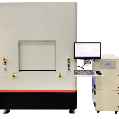 Read More

Contact Us
Recommended Products
-
 Farewell to "Stone Pain"! 1940nm Thulium Fiber Laser: A New Era of Minimally Invasive Urological TreatmentNegotiableMOQ: 10 Combos
 -
Semiconductor-Pumped Erbium Lasers: A New Benchmark for Efficient and Precise Mid-Infrared Light SourcesNegotiableMOQ: 10 Sets
-
1.5μm/2μm Laser Welding: The \"Light\" Solution for Precision Welding of Transparent PlasticsNegotiableMOQ: 1 Set
-
Five-Axis High-Precision Laser Cutting Equipment: The Ultimate Solution for Precision Processing of High-End Transparent MaterialsNegotiableMOQ: 1 Combo
-
Precision, Efficiency, and Cross-border Empowerment of 1940 nm Continuous and Quasi-Continuous Fiber LasersNegotiableMOQ: 10 Sets
-
1470&1940nm Dual-wavelength Fiber LaserNegotiableMOQ: 10 Sets
-
Unlocking New Possibilities in Medical Lasers: Technology and Applications of Flashlamp-Pumped Erbium/Holmium LasersNegotiableMOQ: 10 Pieces
-
Veterinary Thulium Fiber Laser Therapy System: 1940nm Minimally Invasive Solution for Safer Pet CareNegotiableMOQ: 10 Pieces
-
Dual-Wavelength Fiber Laser for Medical Aesthetics: 1550nm + 1927nm, Synchronous Improvement of Deep and Superficial Skin Layers in One TreatmentNegotiableMOQ: 10 Units
-
✨ Rayever | Mid-IR Laser Core Materials PortfolioNegotiableMOQ: 10 Pieces
-
1940nm Thulium Fiber Laser: Say Goodbye to Open Surgery for Your Furry FriendsNegotiableMOQ: 10 Sets
-
Rayever Photoelectric Medical Optical Fibers, the "Energy Lifeline" of Laser MedicineNegotiableMOQ: 100 Sets
-
YFL-2000 Portable Fiber Laser,Extreme Environment "Mobile Operations"!NegotiableMOQ: 10 Units
-
0.8~2.1μm Full Band Coverage! Rayever Photoelectric Fiber Components, Building the Core Foundation for Laser SystemsNegotiableMOQ: 100 Sets
-
Breaking Material Limits! Large-Size Broadband Transparent Ceramic WindowsNegotiableMOQ: 100 Units
-
The Versatile 1550nm Fiber Laser: A Cross-Field Powerhouse From Aesthetic Anti-Aging to Precision ManufacturingNegotiableMOQ: 1 Set
-
Medium Wave 3 ~ 8μm LaserNegotiableMOQ: 10 Sets
-
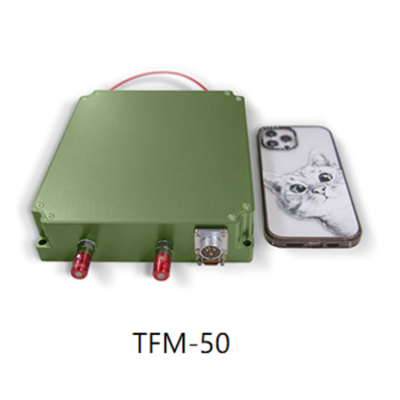
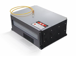
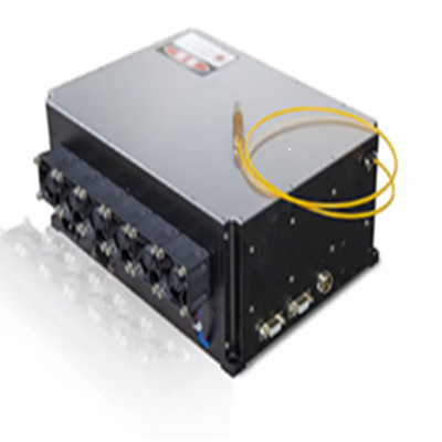
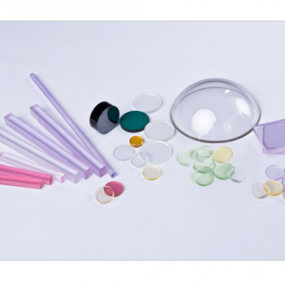
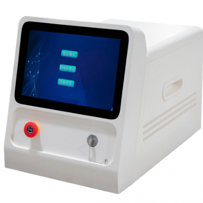
1342nm Solid-state LaserNegotiableMOQ: 1 Set
-
Fiber Optic DevicesNegotiableMOQ: 100 Sets
-
High Power Lightweight and Miniaturized 2-micron Laser ModuleNegotiableMOQ: 1 Set